We have experienced and skilled Engineers to complete the DFM checks and provides complete Front end Engineering services to PCB Manufacturers. PCB orders received from PCB Fab houses are completed quickly and our proven methods will give you the consistency results.
We work along with PCB Manufacturers using the standard Guidelines and customer supplied Guidelines to perform Customer specific DFM checks and produce Panelization.
What we do?
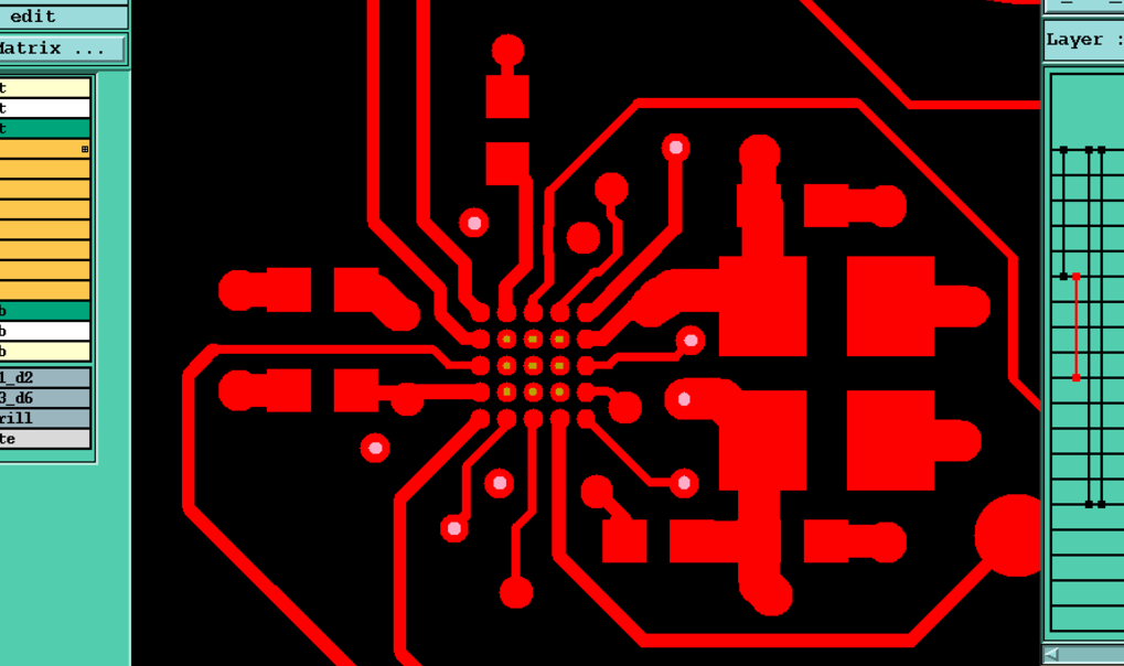
- Recognizing the format of the artwork layers, drilling data, IPC Net list, etc. We are well versed in handling Rigid boards, High layer-count, HDI multilayer’s including blind and buried vias, impedance-control, plated edges/Castellated holes & Edge milling jobs.
- Performing Design Rule Checks, Comparing the IPC net lists with the imported data.
- Configuring nesting of parts on the production panel for best orientation of the part to maximize machining material utilization and machine efficiency. All editing works with complete panelization for single, double sided and multi layer boards.
- Creating tools like Copper, Solder mask, Silkscreen artworks, Drill programs, routing programs, Electrical Test Programs necessary for manufacturing the PCB from the design.
Blind and Buried vias connects between layers of a PCB where space is at a premium. A Blind Via connects an outer layer to one or more inner layers but doesn't go through the entire board. A Buried Via connects two or more inner layers but doesn't go through to an outer layer.
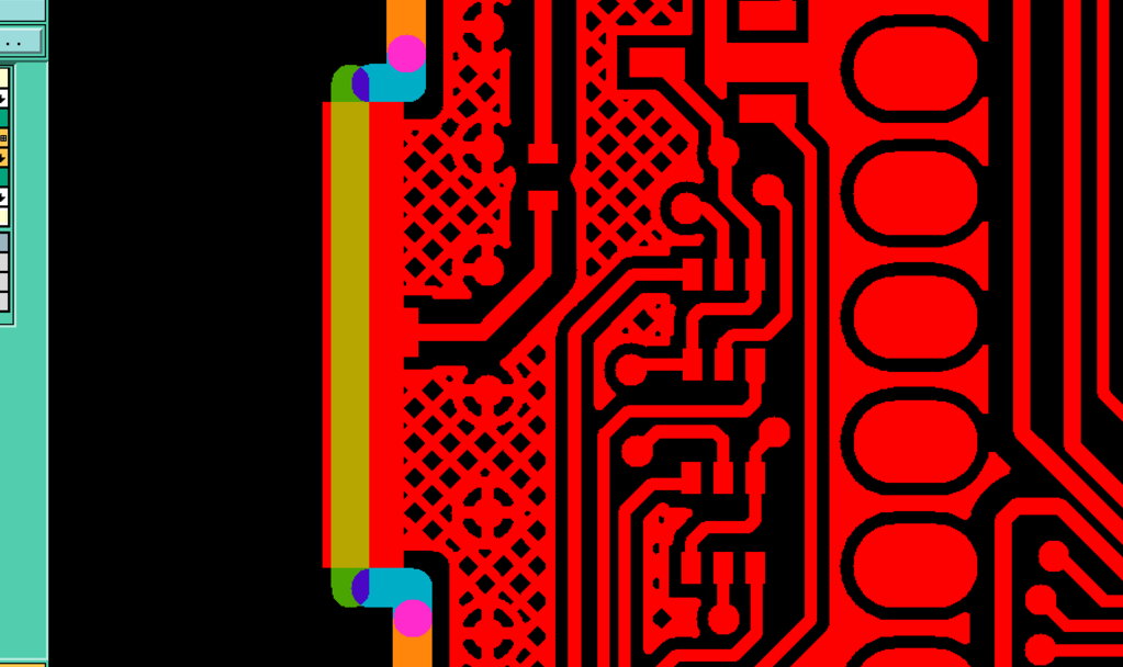
Edge plating is the copper plating connecting the top to the bottom surface of a PCB, running along at least one of its perimeter edges. Edge plating connects copper traces or planes in between layers of the same board and these boards are used in applications like connectors that slide into metal casings.
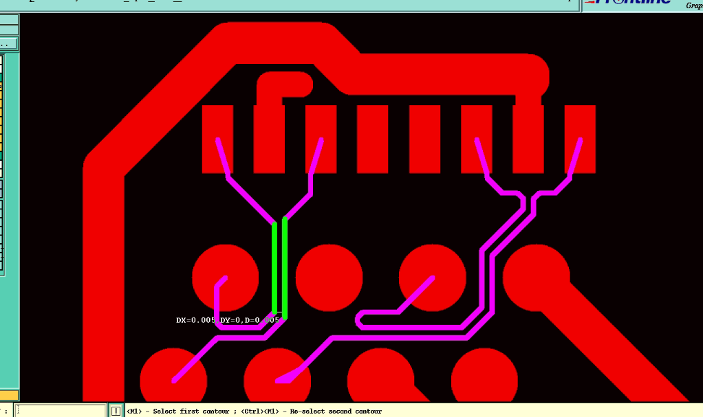
Impedance is the combination of the capacitance and inductance of a circuit when operated at high frequency. Though also measured in Ohms, it is somewhat different than resistance which is a DC characteristic. Impedance is an AC characteristic, meaning that it is related to frequency, resistance is not.


